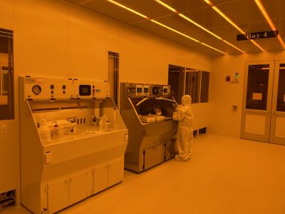
Bay 4: Deposition
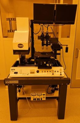
Mask Aligner
OAI Model 200
The OAI Model 200 Mask Aligner is a cost-effective high-performance mask Aligner that has been engineered with industry-proven components in the photolithography industry. It is a highly flexible, economical solution for any mask alignment and UV exposure application. It is enabling photolithography, which is a microfabrication process used to selectively remove parts of a thin film to create a pattern or a design onto a substrate.
The alignment module includes micrometers for precise adjustment along the X, Y, and Z axes. A UV light source at a wavelength of 365 nm delivers focused UV light across the entire wafer. This equipment can reliably create patterns in photoresist at the micron scale using a transmission mask with a maximum of 5 inches in size. The substrate is swiftly leveled to ensure accurate alignment with the photomask and uniform contact across the substrate during contact exposure. The maximum substrate size exposed is 5 inches in diameter.
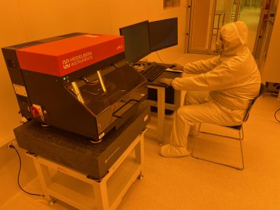
Maskless Aligner
Heidelberg Instruments µMLA System
The tabletop µMLA system is state-of-the-art in maskless technology built on the renowned µPG platform – the most sold tabletop maskless system worldwide. It is a perfect entry-level research and development (R&D) tool for virtually any application requiring microstructures. Typical examples are microfluidics (cell sorting devices, lab-on-a-chip), small-scale mask-writing, micro-optics, microlens arrays, sensors, MEMS, contacting 2D materials, fan-out electrodes, etc.
The substrate size is up to 6x6 inches (150x150 mm) with a minimum feature size of 1.0 µm. The maximum write speed at 4 µm resolution is 90 mm2/min (0.14 sq inch/min) using an LED light source with 365 nm exposure wavelength.
Other Equipment
Wet Processing and Cleaning Stations, Bake Plates, Spin-Coater, Sonicator
There are six wet chemistry fume hoods, a combination of stainless steel and polymer units designed for various chemical processing tasks (cleaning, wet etching, etc.) employed in semiconductor and microelectronic device fabrication.
Hood 1 in Bay Area 4 (Spin Coater-Bake Plate hood) is dedicated to photolithography processes and includes a spin-coater and bake plates for applying photoresist and other polymers. Hood 2 in Bay Area 4 (Developer hood) has all photoresists and is also suited for pattern development, wafer cleaning, photoresist removal, and other processes.